Recently we made a 7-segment display multiplex itself thanks to the magical MAX7219 chip. Today I’ll show you how these chips let you handle a theoretically infinite number of displays. We’re talking about the daisy-chain connection these wonderful chips offer. In a moment you’ll see how, without using more pins, you can connect and control as many displays as you want. Let’s get to it!
Complete series of posts:
No more multiplexing on GPIO! MAX7219 in action part 1
No more multiplexing on GPIO! MAX7219 in action part 2
No more multiplexing on GPIO! MAX7219 in action part 3
MAX7219 – daisy-chain connection
To increase the number of LEDs you can control, you would connect another MAX7219 chip. In the “classic” setup you would allocate a separate CS pin to select the active chip, while data and clock would be connected in parallel to the second chip. That would even make sense, but what if I told you I want to connect 500 chips to drive thousands of LEDs? Find me an STM that has over 500 pins. Tough one…

This is where daisy-chaining comes to the rescue. What is it, and why does it let you handle 500 chips without trouble? I’m glad you asked. A cascade occurs in nature or gardening and is a type of waterfall or fountain. In general, it’s about the flow of water. As a reminder, take a look at the first image from Google of such a formation.
How does this relate to electronic circuits? Notice that a cascade is made of stages. Each such stage is one of our MAX7219 chips. The water represents the data we send into the chain. The top of the waterfall is the first chip. The data (water) flows through it and reaches the next ones, flowing through successive chips in the chain. In the electronic waterfall there’s also a moment of accepting, or more formally, latching the data. After all, what we send to the chips should reach them, not just pass through. Also note that when you introduce a new item of data, all older ones shift forward by one, so when you write something for element no. 0, in a moment it will reach element no. 1. We don’t want that one to perform the same task as well…
To control what the chips latch, we use the regular CS. The MAX7219 will accept the data it currently holds only if a rising edge appears on the CS pin. Returning to the waterfall metaphor, the CS could be a frog that eats the bug (the data) floating by :). What does the connection of several MAX7219 chips look like? The documentation will help.
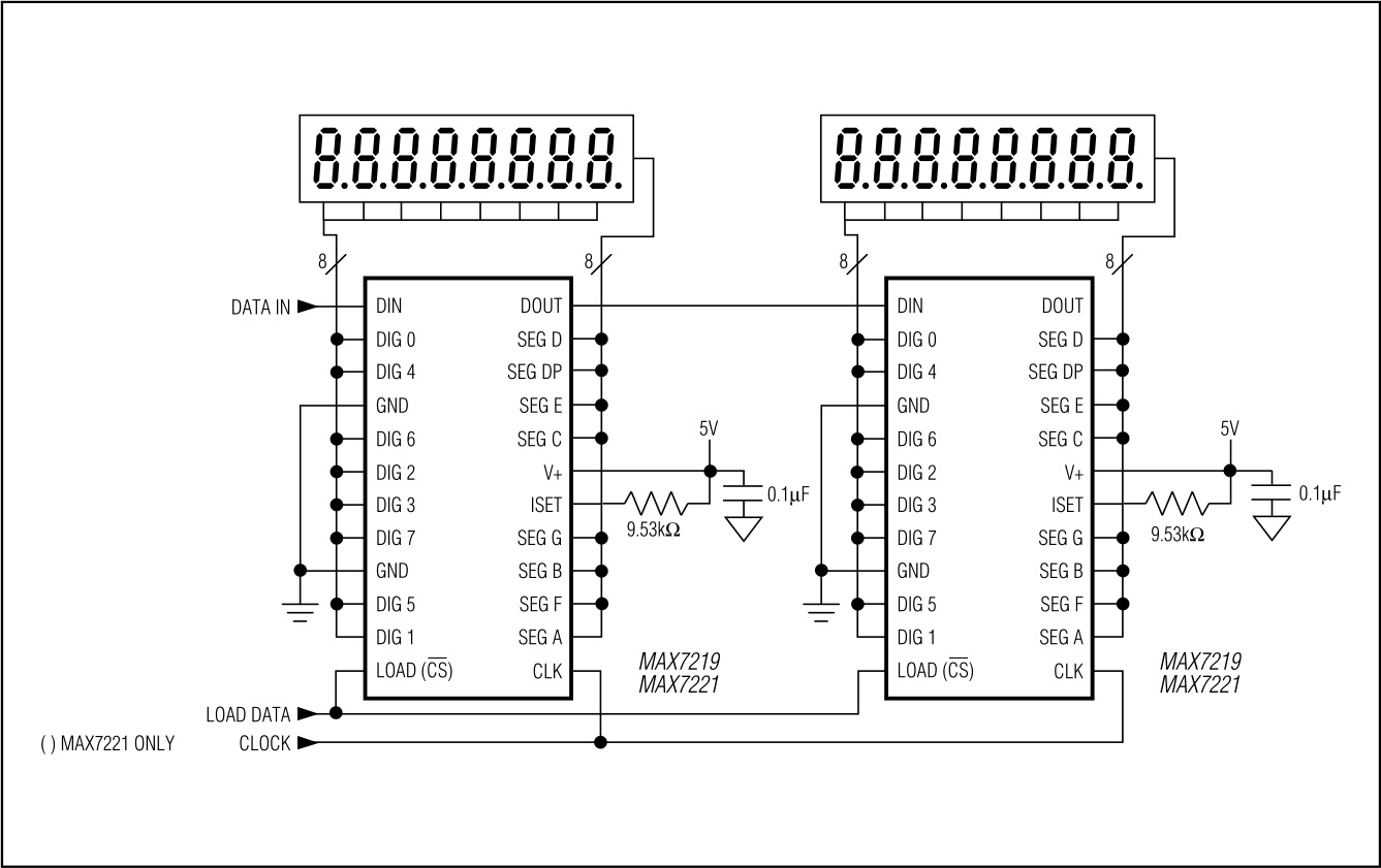
As you can see, on the MCU side there are only three signals (on the left):
- DATA IN, i.e., MOSI of the SPI interface
- CLOCK, i.e., SCK
- LOAD DATA, i.e., CS
The clock and CS are connected in parallel to each chip. The DATA IN of each subsequent chip is connected to the DATA OUT of the preceding one. It’s on this pin that chips present historical data to be passed further along.
Feeding data into the chain
A very important aspect is understanding how to “address” data. We already know how such addressing works, because we’re familiar with WS2812B LEDs, which I described in another series (Addressable WS2812B LEDs on STM32 part 1). In that chain the difference was that latching depended on timing, and the principle of feeding data was reversed (or rather, logical). There, after an LED received its data, it remembered it and forwarded only the next data on its output, which no longer concerned it. So we wrote data into that chain in order from 0 to n.
With the MAX7219 it’s different. Latching happens when the CS pin goes high. The chips don’t keep anything for themselves; they pass along everything that comes into their hands like monkeys, holding only the most recent thing they got for a moment. In this case, the first thing you need to write into the chain is the information for the last chip, then the second-to-last, and so on up to the zeroth. Let me illustrate this with a logic analyzer trace on a live example. I have four chips daisy-chained, which gives me a total of 5 points where data can appear:
- SDIN0
- SDOUT0<->SDIN1
- SDOUT1<->SDIN2
- SDOUT2<->SDIN3
- SDOUT3
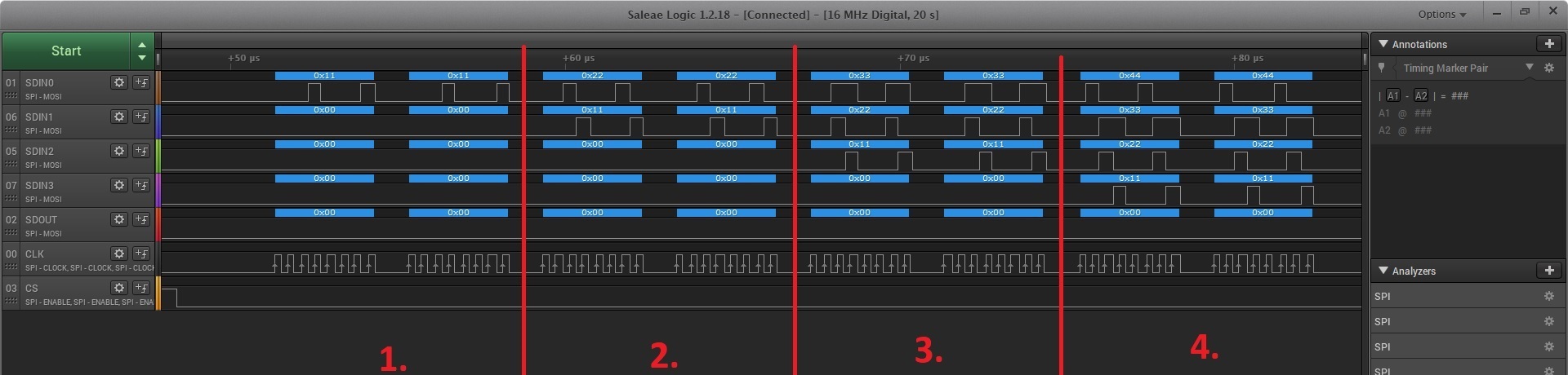
The bolded names are the ones I used in the waveform image. I split the trace into four sections because, I’m sending four messages. One for each chip. MAX7219 accepts data in 2-byte packets, hence I’m sending a total of 8 bytes.
To make the analysis easier, I’m sending data packets that represent successive steps, i.e., 0x11 for the first step, 0x22 for the second, etc.
- The first packet 0x11 reaches the SDIN input of chip zero. The data is stored in the chip but not latched yet—it’s waiting for a rising edge on the CS pin.
- No edge appeared, but another packet arrived at SDIN0—0x22. The first chip in line needs to make room for the new data, so it pushes the old one to its SDOUT, which in turn goes to the SDIN of chip number 1. Now two chips are waiting for a rising edge on the CS pin.
- Again, the edge did not appear, and a new set of data showed up once more. Each of the previous chips makes room for the new data by pushing the old to its SDOUT. 0x11 goes to chip number 2, 0x22 to chip number 1, and the freshest data, 0x33, is now in chip number 0. Now three chips are waiting for a rising edge on the CS pin.
- And surprise—the edge still didn’t show up at the CS pin. The whole sequence of chips passing along their data starts again. Each of them forwards what it currently held. As a result, 0x11, which was introduced into the chain first, reached chip no. 3, we have 0x22 on chip no. 2, 0x33 on no. 1, and 0x44 at the beginning.
It didn’t fit on the plot, but after all this, CS finally goes high. At that moment, the data that each chip was holding is latched, and the corresponding operations are only now performed by the chips.
Handling the chain in the library
The library has supported daisy-chaining from the very beginning, and handling multiple chips is implemented in the function:
MAX7219_STATUS MAX7219_SendToDevice(uint8_t DeviceNumber, uint8_t Register, uint8_t Data)
The whole trick is to operate on a buffer whose size corresponds to the number of chips in the chain. With four chips, the buffer size is 8 bytes (remember that data must be in 2-byte packets). First, the offset of the device you want to write to is determined. Then the entire buffer is zeroed. As you remember from the previous post, zero is the No-op operation, i.e., no operation. Writing it to a chip changes nothing.
In the next step, you need to write the register and value data into the buffer in accordance with the computed offset. Remember the nature of the chain: if you want to write to the first element, you send it as the last value, and vice versa. If you’re writing to the last element, send it into the chain first.
After filling the buffer, just transfer it over SPI. Done. The given data has been written to the chip you wanted to address.
Chain in action
You’ll find demonstrations of the chain in action on 7-segment displays in the video below. Unfortunately, readily available modules are not friendly for physically combining displays. They have a piece of PCB on both sides, which prevents perfect alignment of the displays.
Summary
I hope I’ve clearly explained how daisy-chaining works. This technique is often used in shift registers, which is what the MAX7219 chips discussed today essentially are. The well-known WS2812B LEDs also use a similar mechanism, which makes them incredibly configurable. In the next part, I’ll deal with matrix displays. I’ll daisy-chain them and also combine them into a single larger display, which can be easily controlled from a graphics library!
You can find the complete project along with the library on my GitHub as usual: link
Podobne artykuły





0 Comments